Hardware

The boards the software was written for.

The boards are designed the same way the software is analysed: in KiCad from netlist-as-code, with ERC, DRC and schematic parity as release gates, and a test-coverage workbook per board. Every part carries an LCSC code so the BOM and the pick-and-place file can go straight to a fabricator. The 3-D views below are KiCad's own renders of the real boards, not illustrations.

These are designed and in the pipeline: files released, parts sourced with an LCSC code on every line, and boards moving through fabrication and assembly. This page does not track which stage each one is at in a given week - ask if a particular board matters to you.

Not for sale yet Every board below is designed and gated, and in the pipeline.

A graph of the Z-Stack Controller Carrier at the centre, linked to the four applications that analyse it, to the manufacturing files that come out of it, and to the other boards that take the same route
Every board takes the same route, and the worked figures everywhere else on this site come from the one in the middle.

Z-Stack Controller Carrier rev A

In the pipeline

The board every other page on this site is analysed against.

A focus-stacking controller: an ESP32-S3 development kit drives a stepper through a plug-in driver module, advances the stage one step at a time, and fires an isolated camera shutter at each position. Panel buttons, an encoder, a 20x4 I2C display and a bottom limit switch complete it. This is the board used as the worked example throughout the software pages - the coverage analysis, the EMC findings and the test plan are all this board.

Test fixtureA bed-of-nails fixture plate is drawn for this board, located from its mounting holes, with the probe positions taken from the coverage analysis. Designed, not yet machined.
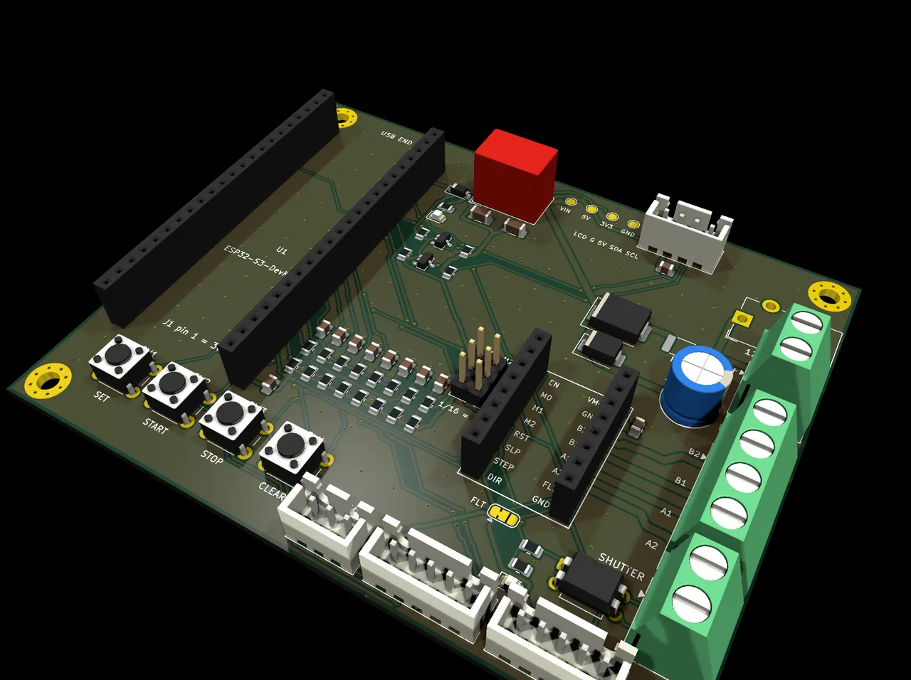
HostESP32-S3-DevKitC on a socket, USB to the PC
Motionplug-in stepper driver module, 1/16 microstep, A1/A2/B1/B2 to screw terminals
Cameraisolated shutter output through a PC817 optocoupler
PanelSET, START, STOP and CLEAR buttons, an encoder input and a 20x4 I2C display header
Supply12-24 V DC, barrel jack or screw terminal
Test pointsVIN, 5V, 3V3 and GND brought out
ReleasedGerbers, Excel BOM, STEP, design review and a bed-of-nails fixture plate
Rev A. The dev kit sockets along the top edge, the stepper driver module plugs into the centre, and the shutter optocoupler sits bottom right beside its terminal. The four panel buttons run along the left edge, and VIN / 5V / 3V3 / GND test points sit by the power input - the same test points the coverage analysis checks a probe can reach.

USB Oscilloscope 8 single-ended / 4 differential

In the pipeline

Eight channels sampled together, over one USB cable.

A TI ADS8588S samples eight inputs simultaneously at up to 200 kS/s per channel, read by a plug-in Teensy 4.1 and delivered over a single USB cable. Channels pair into four differential inputs in firmware.

Board150 x 100 mm, 1.6 mm
Front endTI ADS8588S, 16 bit, simultaneous sampling
Rateup to 200 kS/s per channel
HostTeensy 4.1, firmware 2.0.0, USB Dual Serial
Revisionrev B, design review issue 3
Reads intoSignalScope, HardwareRTD, Excel
The 8 SE / 4 DIFF board, rev B - KiCad's render of the real layout. The Teensy 4.1 plugs into the sockets at the right; the ADS8588S and its input conditioning fill the left half.

4-Channel USB Oscilloscope the cost-down

In the pipeline

The same idea, four channels, and parts you can actually buy.

A deliberate cost-down of the eight-channel board, derived from its rev A. The AD7606C-16 that rev A used is not stocked by LCSC or JLC, so this drops in the pin-compatible classic AD7606 instead: four BNC inputs sampled together, two pairs usable as differential channels, read by the same plug-in Teensy 4.1.

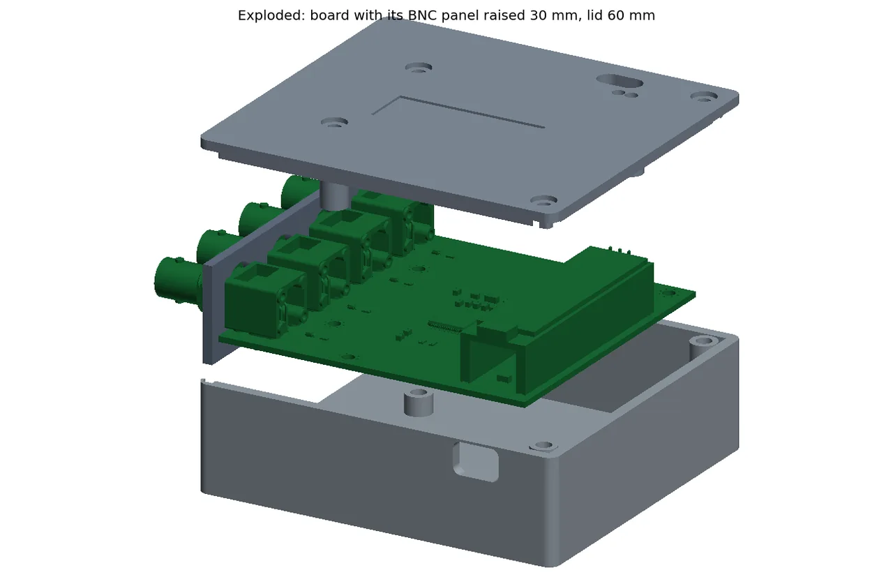
Enclosure3-D printed base, slide-in BNC panel and lid. 98 x 90 x 30.5 mm outside. Designed, not yet printed.
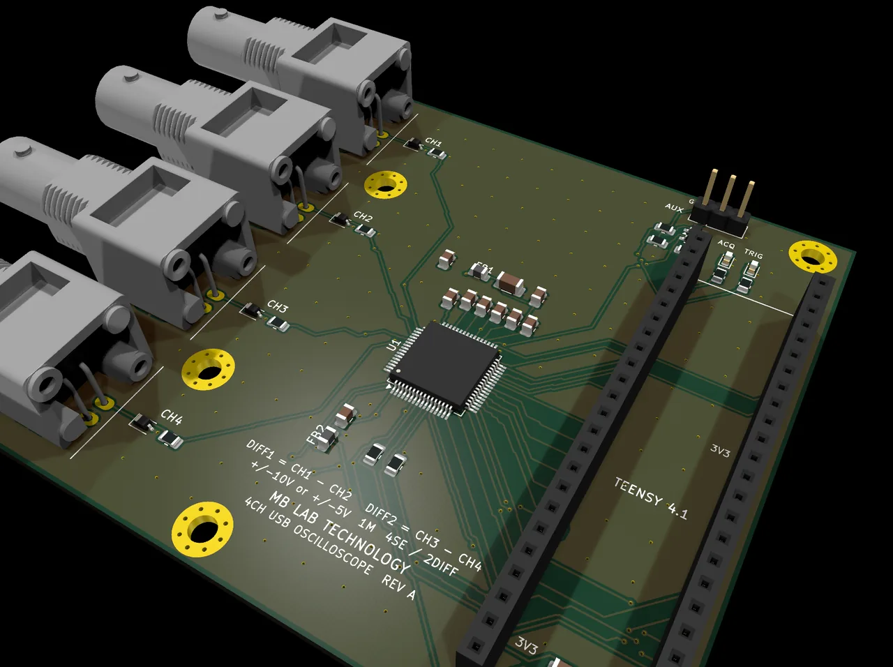
Board84 x 81 mm, 2 layers, 39 placed parts
Inputs4 x right-angle panel BNC, 1 MOhm, +-10 V or +-5 V
DifferentialDIFF1 = CH1 - CH2, DIFF2 = CH3 - CH4
Front endAD7606, 16 bit, up to 200 kS/s per channel
Bandwidthabout 22 kHz at +-10 V - the AD7606's fixed filter
Parts costabout $32 of LCSC parts at one-off prices, of which the four BNCs are $23.51, plus the Teensy
The four-channel board, rev A. The right-angle BNCs sit on the left edge so they pass straight through the case panel.
The enclosure, exploded: base, the board with its slide-in BNC panel, and the lid. Drawn in FreeCAD as PartDesign bodies driven by a spreadsheet of named dimensions, so any size can be retyped.

Mains Power Monitor 3 phases and neutral

In the pipeline

Eight mains channels, sampled on the same edge, across an isolation barrier.

A hot front end that floats at neutral and divides L1, L2, L3 and PE into an AD7606; an isolation barrier of two extra-wide-body digital isolators and an isolated DC/DC; and a SELV side where a second AD7606 reads four current transformers on the same conversion edge. A plug-in Teensy 4.1 reads both converters and serves USB and Ethernet. Voltage and current are therefore simultaneous rather than interleaved, which is what makes real power on three phases worth calculating.
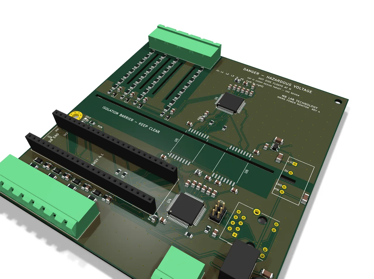
Channels8 sampled together - L1, L2, L3, PE on the hot side, four CT secondaries on the SELV side
Converterstwo AD7606, one per side, on a common conversion edge
Isolationtwo extra-wide-body digital isolators and an isolated DC/DC between the two sides
Hostplug-in Teensy 4.1, USB and Ethernet
Mains inputDinkle DB3ERC-7.62-5P, 1 kV, L1 L2 L3 N PE from the top edge
CT input4 pairs on a 5.08 mm pluggable, bottom edge
Auxiliary supply7-30 V DC on a pluggable terminal
GatesERC 0, DRC 0, parity 0, ICT 69 of 69 nets (28 waived)
ReleasedGerbers, BOM, STEP, firmware 1.0.0, and EMC, validation and test-specification project files
Rev A. The hot front end is the section that floats at neutral, with the mains terminal along the top edge; the isolation barrier runs across the middle, and the SELV side carries the second converter, the current-transformer inputs and the Teensy. Machine routed, and the bench bring-up is still ahead of it.

ESP32-S3 PLC 12 DIO / 24 AI

In the pipeline

The board MBLT PLC was written to drive.

A carrier that turns an ESP32-S3 development kit into a usable small PLC: twelve digital I/O, twenty-four analog inputs through a 24-bit ADC module, and a wide-input buck-boost supply so it will run from whatever the machine has. MBLT PLC describes this board in full, rev A and rev B, as a build target.

Board260 x 150 mm, 1.6 mm
HostESP32-S3-DevKitC-1 v1.1 or YD-ESP32-S3 on 1x22 sockets
AnalogADS1256 24-bit 8-channel ADC module, 24 AI
Digital12 DIO
SupplyPololu S18V20F5 buck-boost, 2.9-32 V in, 5 V 2 A out
Programmed byMBLT PLC - ladder, FBD, SFC, ST, IL or C/C++
Also in the projecta PWM adaptor board, and an LP5 laser-made prototype of the carrier
Rev B. The dev kit and the ADS1256 module drop into sockets rather than being soldered down, so a failed module is a two-minute swap instead of a rework job.

SoundCard Scope Probes isolated differential front end

In the pipeline

Mains voltages into an ordinary sound card, safely.

An isolated differential probe and a two-channel interface that let SignalScope measure anything from logic levels up to 1000 Vrms through a sound card's line input. The isolation is a TI AMC3311 reinforced isolation amplifier behind a symmetric divider - one PCB, three populations for three voltage ranges.

EnclosureTwo 3-D printed cases - a probe pod case with panel binding posts, and an interface case with light pipes for the indicator LEDs. Designed, not yet printed.

Probe pod32 x 98 mm, TI AMC3311 reinforced isolation amp
RangesLV +-108 V, MAINS +-729 V (230/400 V), HV +-1459 V
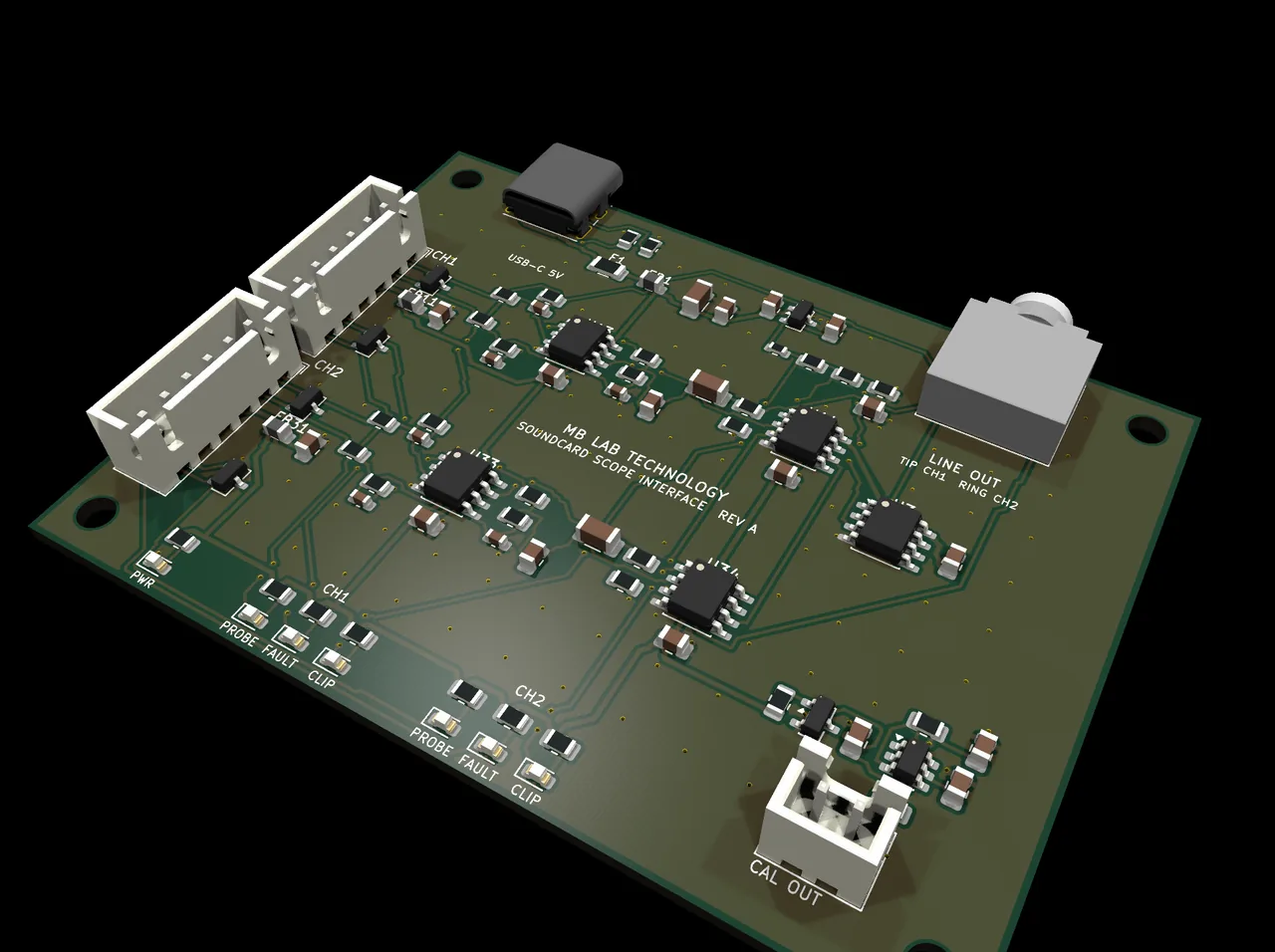
Interface80 x 60 mm, USB-C powered
Per channeldifference amp x0.5, 32.5 kHz low-pass, AC-coupled line out
Output3.5 mm jack - tip CH1, ring CH2
IndicatorsCLIP / FAULT / PROBE LEDs, 0 / 2.500 V CAL OUT
Reads intoSignalScope, through the sound card
The probe pod, 32 x 98 mm. The isolation barrier runs across the middle of the board; the 8 + 8 resistor divider on the input side is what sets which of the three populations a board becomes.
The two-channel interface, 80 x 60 mm. USB-C for power only, a difference amplifier and 32.5 kHz filter per channel, and the calibration output that lets the scope check its own scaling.

USB8Serial eight RS-232 ports

In the pipeline

One USB cable, eight real COM ports with full modem control.

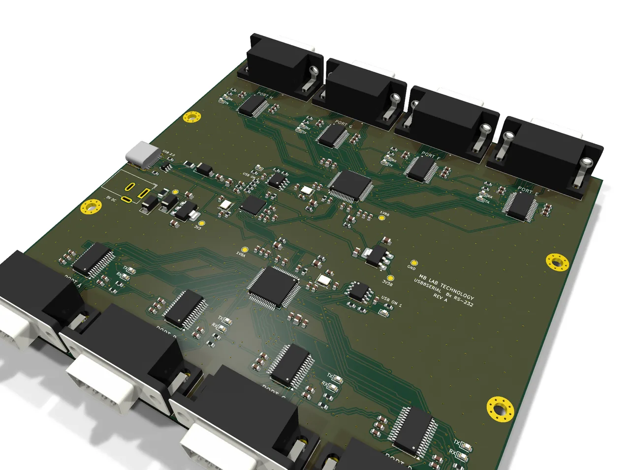
A 138.2 x 131.6 mm two-layer board that turns one USB 2.0 High-Speed connection into eight RS-232 ports. A Microchip USB2514B hub feeds two FTDI FT4232HL bridges; each UART drives its own TI MAX3243E and a male DB9 wired as DTE, exactly like a PC's COM port. Ports A to D leave one long edge and E to H the other. It runs from USB, or from a 5 V adapter when the port cannot supply what eight transceivers want.
Ports8 x RS-232, full modem control, DB9 male wired as DTE
HubMicrochip USB2514B
Bridges2 x FTDI FT4232HL - the host sees eight standard FTDI serial ports
Transceivers8 x TI MAX3243E
ConnectorsUSB-C (HRO TYPE-C-31-M-12), 8 x Wurth 618009231221 right-angle DB9 with 4-40 screw locks
SupplyUSB, or a 5.5 x 2.1 mm jack when the port cannot carry it
Board138.2 x 131.6 mm, two layers, 4 mounting holes
Test points+5V, +3V3, VCOREA, VCOREB, GND, +3V3B
GatesERC 0, DRC 0 errors with 5 warnings, 0 unconnected, parity 0, test gate pass
Rev A. The USB-C and the optional 5 V jack are on the left edge, the hub and the two four-port bridges sit across the middle, and the eight DB9s leave both long edges - A to D on one side, E to H on the other, so a rack of eight instruments can be cabled from either direction.

USB4Serial four RS-232 ports

In the pipeline

The same idea, half the size, no hub in the way.

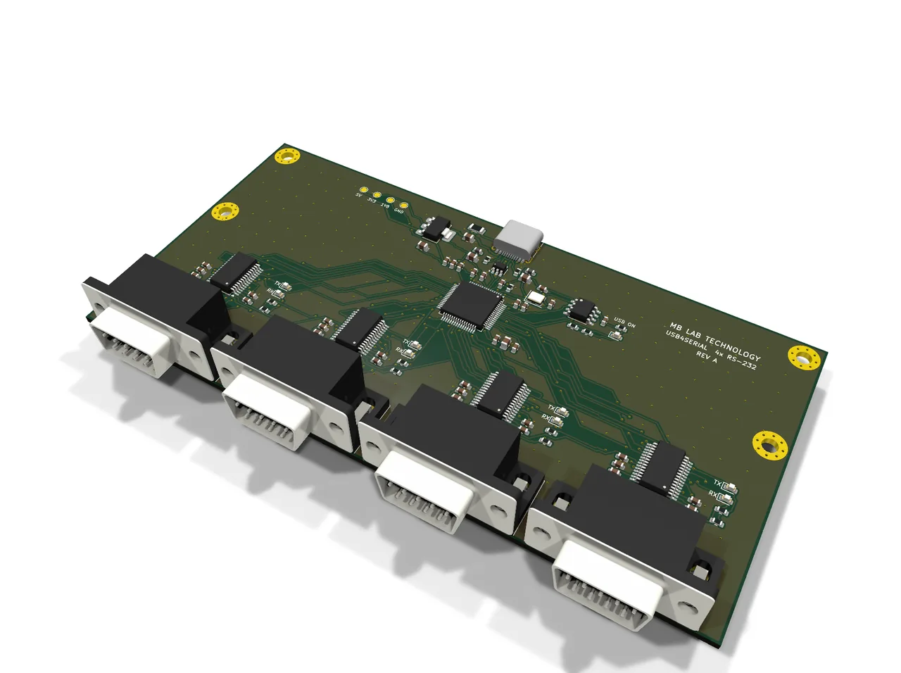
A 138 x 69 mm two-layer board that turns one USB 2.0 High-Speed connection into four RS-232 ports with full modem control. One FTDI FT4232HL provides all four UARTs, each driving its own TI MAX3243E and a male DB9 wired as DTE. The board is powered from USB and the host sees four standard FTDI serial ports - no hub, no driver to hunt for.
Ports4 x RS-232, full modem control, DB9 male wired as DTE
Bridgeone FTDI FT4232HL for all four UARTs
Transceivers4 x TI MAX3243E
ConnectorsUSB-C (HRO TYPE-C-31-M-12), 4 x Wurth 618009231221 right-angle DB9 with 4-40 screw locks
Supplybus-powered from USB
Board138 x 69 mm, two layers, 4 mounting holes
Routing0.2 mm tracks at 0.15 mm clearance, so a track leaves the centre of a 0.5 mm-pitch LQFP pad without violating the gap to the next one
GatesERC 0, DRC 0 errors with 2 warnings, 0 unconnected, parity 0, test gate pass, design review DR-U4S-A
Rev A. One bridge in the centre, four transceivers around it, and the four DB9s along the front edge. All 32 UART pins leave the FT4232HL on its left, right and bottom sides, which is what keeps the board to two layers.

Roulette Sample Board the board the apps demonstrate on

In the pipeline

A sample product, so a real product does not have to play that part.

A 100 x 100 mm two-layer demonstration board: an Arduino Nano on sockets drives a roulette wheel of 37 LEDs and three status LEDs through five 74HC595 shift registers, reads four push buttons and sounds a buzzer. It exists so the apps, the ICT fixture and the documentation have something to be demonstrated on that is not the Z-Stack carrier - which is a real product and should not have to be the worked example for everything.

Test fixtureA bed-of-nails fixture plate is drawn for this board, located from its mounting holes, with the probe positions taken from the coverage analysis. Designed, not yet machined.

HostArduino Nano on 2 x 1x15 sockets, 2.54 mm
Outputs37 wheel LEDs and 3 status LEDs through five 74HC595 shift registers
Inputsfour push buttons; a buzzer for the result
Expansion1x6 header - GND, +5V, SCL, SDA, A3, A2
Board100 x 100 mm, two layers
Test accessICT reaches all 109 nets from the bottom on 109 probes, every one a flat pad on the 100 mil class
Coverage92.4 % combined, 81.8 % joint - AOI 78.2 %, ICT 58.3 %, flying probe 57.2 %. Pre-fixture estimates from the design data, not measured
GatesERC 0, DRC 0, 0 unconnected, parity 0; firmware compiled, not yet run on hardware
Rev A. The wheel of 37 LEDs with the Nano socketed in the middle, the five shift registers feeding it, and the buttons and buzzer along the edge. The reason it is on this page: PCB Test Analysis, the fixture generator and the ICT work all need a board to point at, and this one was designed to be pointed at.

IR Detector, SMT 35 to a panel

In the pipeline

A reflective sensor small enough that the panel is the interesting part.

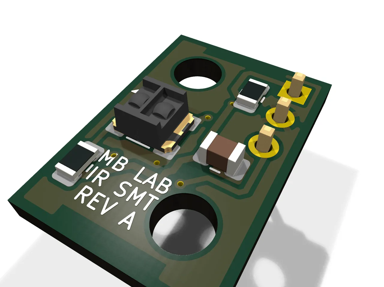
The all-SMD sibling of the TCRT5000 board. A Sharp GP2S700HCP - a 4 x 3 x 2 mm leadless package holding a 950 nm IR LED and a phototransistor side by side - replaces the through-hole sensor, so every part except the hand-fitted header can be placed by the assembler. The interface is unchanged: VCC, GND and an analog OUT on a three-pin header, 3.3 to 5 V.
SensorSharp GP2S700HCP, 950 nm, 4 x 3 x 2 mm leadless
Interface1x3 header - VCC, GND, analog OUT, 0 V to VCC
Supply3.3 V to 5 V
Output impedance10 kilohm
Board11.4 x 16.5 mm, two M3 holes
Panel35 boards to a 100 x 100 mm panel on mouse-bite tabs
Assemblyfour parts placed on the top side; the header is hand-fitted from the back after depanelling, so the front stays flat behind an enclosure window
Test accessevery net has a bottom-side test pad - the sensor is SMD and the header sits inside the fixture's 3 mm edge keep-out
GatesERC 0, DRC 0, issue 2
Rev A, and the whole board is 11.4 x 16.5 mm - the sensor, three passives and a header.
The reason the outline is that exact size: 35 of them share one 100 x 100 mm panel on mouse-bite tabs, placed in one pass. The tabs sit at x = 5.5 mm, the only line clear of copper on both short ends.

IR Detector / Locator 21 to a panel

In the pipeline

The same sensor in through-hole, for when the part has to be the cheap one.

A small board that sees objects in front of it. A Vishay TCRT5000L shines 950 nm infrared forward and a phototransistor beside it measures how much comes back; the board turns that into an analog voltage on a three-pin header. It is sized for an enclosure - two M3 holes - and for the panel: 11.4 x 28 mm is what lets 21 boards share one 100 x 100 mm panel.
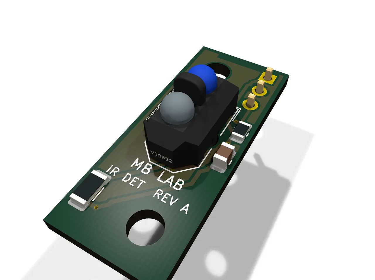
SensorVishay TCRT5000L, 950 nm, through-hole
Interface1x3 header - VCC, GND, analog OUT, 0 V to VCC
Supply3.3 V to 5 V
Output impedance1.2 kilohm
Board11.4 x 28 mm, two M3 holes
Panel21 boards to a 100 x 100 mm panel on mouse-bite tabs
Varianta cost-down BOM against the SMT board, which is the other way of buying the same measurement
GatesERC 0, DRC 0, issue 1
Rev A. The TCRT5000L stands proud at the front; the header is fitted from the back so the face stays flat against a window.
21 up on a 100 x 100 mm panel. Fewer to a panel than the SMT board because the part is taller and the outline longer - which is most of the cost difference between the two.

Buck-Boost 5 V Regulator BB5V

In the pipeline

A drop-in supply for everything else on this page.

A small carrier for the Pololu S18V20F5 buck-boost module, so one supply design can be dropped into any of the boards rather than redesigned each time. Takes whatever the bench or the machine offers and gives back a clean 5 V.

ModulePololu S18V20F5, 2.9-32 V in, 5 V 2 A out
Why buck-boostthe input can sit above or below 5 V and the output does not care
The BB5V carrier - a drop-in footprint for the regulator module, with the input and output terminals brought out.

GPIB-USB Adapter IEEE-488 to a COM port

In the pipeline

The instruments that are too good to replace and too old to reach.

A two-layer adapter that plugs straight into an instrument's GPIB receptacle - or the piggyback side of a GPIB cable - through a right-angle 24-way plug. An Arduino Nano on sockets is the bus controller and the USB port; TI's SN75160B and SN75161B give the bus its 48 mA drivers, receivers with hysteresis and terminations. On the PC it is one COM port, speaking either the MB Lab device profile - so HardwareRTD puts a reading from a 1980s meter into an Excel cell with nothing else installed - or the Prologix '++' command set, for tools that already expect it.

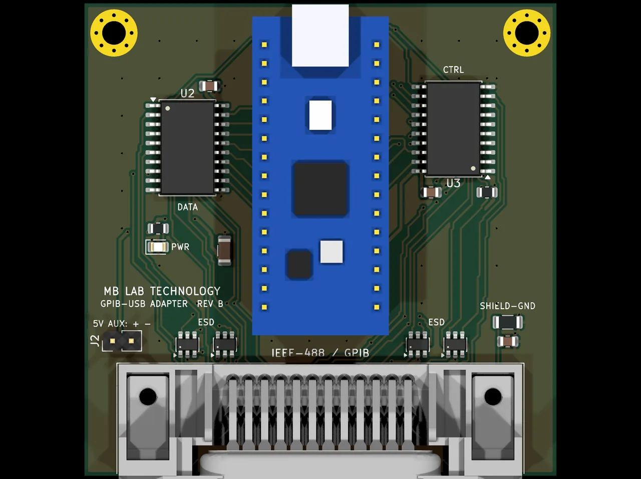
Board64 x 64 mm, two layers
BusIEEE-488 / HP-IB, all 16 lines, 24-way right-angle plug
TransceiversSN75160B data, SN75161B management and handshake
Protectionfour TPD4E1U06 arrays across all 16 bus lines
Host sideArduino Nano on sockets - one USB serial port
GatesERC 0, DRC 0, parity 0, 38 of 38 nets with ICT access
RevisionRev B, 20 October 2026 - the ESD arrays came out of its own design review
The adapter on its plug. The grey body at the front is the 24-way GPIB connector with its jack screws, so the board hangs off the back of the instrument rather than needing a cable; the blue module is the Nano on sockets, and the two wide chips either side of it are the data and control transceivers, marked DATA and CTRL on the silk.
From above, with the four ESD arrays visible as small parts flanking the connector - one for every four bus lines, which is the change that made this Rev B. SHIELD-GND is a pad rather than a track, so the cable screen is tied where you decide it should be.

Scale Interface ESP32, HX711 and a touch display

In the pipeline

Any strain-gauge scale, as an instrument on the network.

A weighing front end that turns a platform of load cells into something the rest of this family can read. A DOIT ESP32 DevKit plugs into sockets; the HX711 24-bit converter, the four-cell combiner, the power path, a Nextion touch-display port, TARE and ZERO inputs and an opto-isolated set-point output are on the board. It takes four 3-wire half-bridge cells summed into one bridge, or a single full-bridge cell, plus a second bridge on the converter's other channel - and answers SCPI over USB and over Wi-Fi, which is what puts it on a bench beside everything else here.
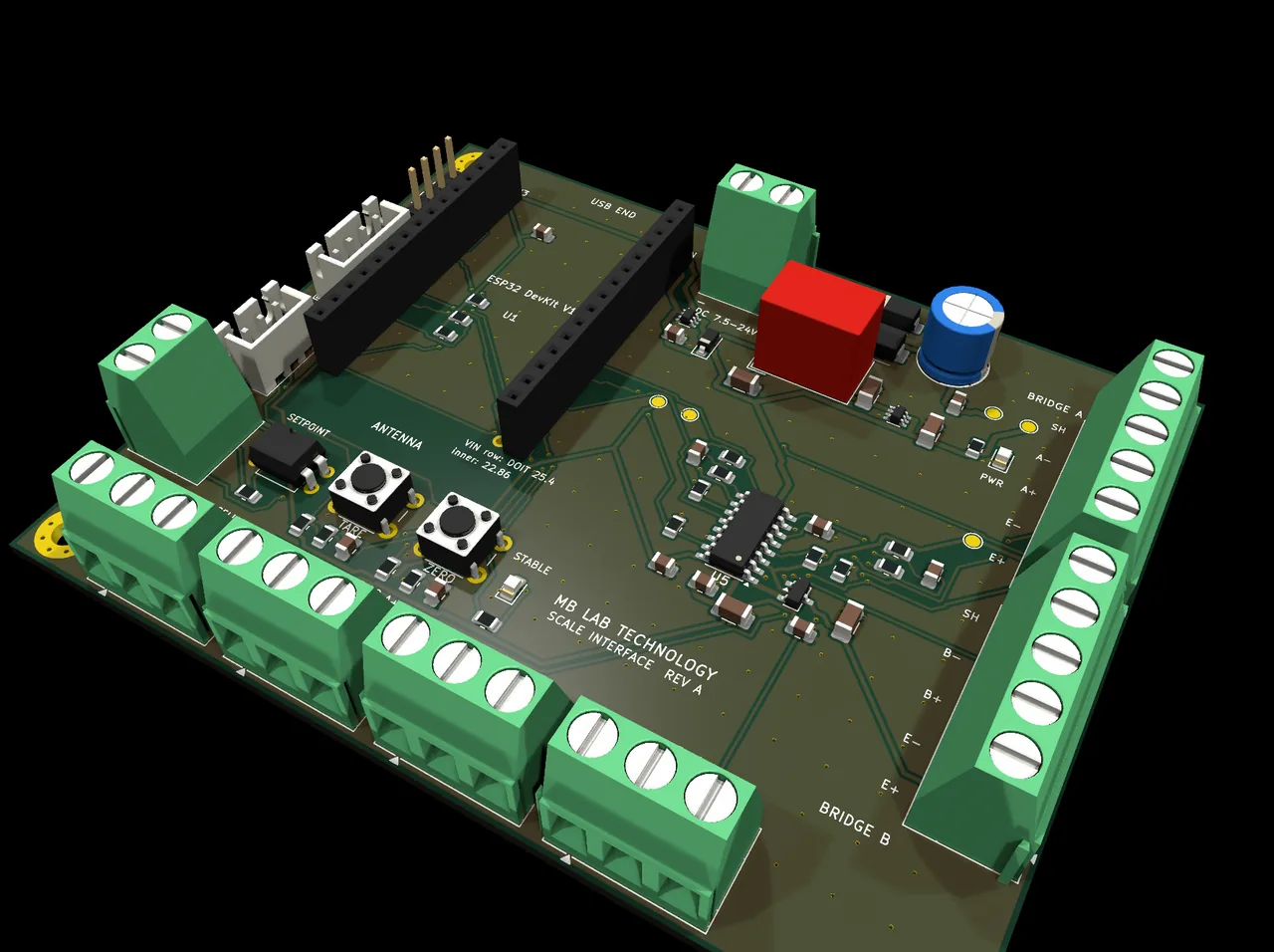
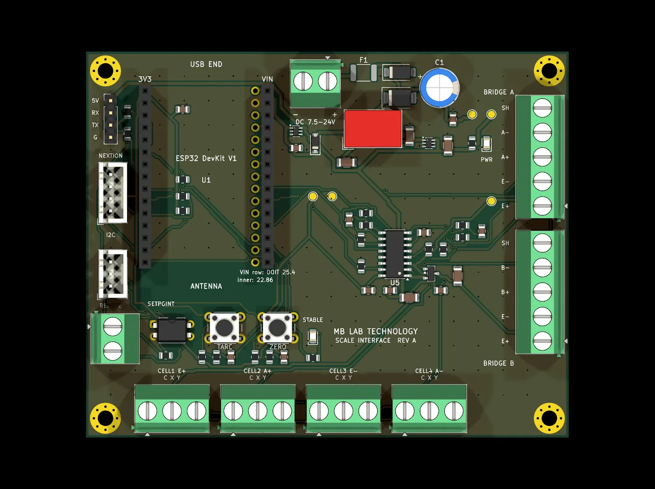
Board100 x 80 mm, two layers
ConverterHX711, 24-bit, two channels
Inputsfour 3-wire half-bridge cells combined, or one full bridge; a second bridge on channel B
ControllerDOIT ESP32 DevKit V1 on sockets
OutSCPI over USB and Wi-Fi, Nextion display on UART2, opto-isolated set point
Supply7.5 to 24 V DC, fused
GatesERC 0, DRC 0, parity 0, 44 of 44 nets with ICT access
RevisionRev A, 20 October 2026
The four green terminal blocks along the front edge are the load cells, one each, labelled with the three wires a half-bridge cell brings; the two down the right are the full-bridge inputs. The two buttons are TARE and ZERO, where an operator can reach them.
From above. The devkit's sockets run up the middle with the antenna keep-out marked beside them, the Nextion and I2C headers are on the left, and the supply comes in top right through a fuse. The board is laid out so that every screw terminal faces out of the enclosure.

RGB LED + Buzzer Shield for Arduino UNO

In the pipeline

The small one, and the one worth learning from.

An Arduino UNO shield with addressable LEDs and a buzzer. It is the simplest board here, which is exactly why it is the one used to demonstrate the whole flow end to end - netlist-as-code, generated schematic, ERC and DRC gates, test coverage, Gerbers and a JLCPCB-ready BOM.

Board114.3 x 53.34 mm - the UNO shield outline
FitsArduino UNO and compatible headers
The shield, with the UNO header outline. Small enough to read the whole layout at a glance, which is what makes it a good worked example.

What is deliberately not here

Someone else's work, until it is credited properly.

A KiCad conversion of a third-party instrument design sits in the same folder as these boards and is deliberately absent from this page. It is not mine. The intention is to build on it and credit it in full, and until that is done properly it does not belong on a page headed "hardware we are building".

Being built now

The set is not only software.

The applications specify a fixture, a sequence, a bench and an enclosure. These are those things being built: the instrument a fixture bolts into, the tester that runs the functional leg, the sequencer that drives it, and the printer that makes the parts. None can be downloaded or bought yet, and none of them has anything to photograph. They are here because each one closes a gap you can already see in the pages above, and because saying what is coming is more useful than letting it arrive as a surprise. No dates — a date I miss is worse than no date at all.

Test equipment

In-circuit test equipmentBeing designed

The tester that the fixture files already describe.

What already exists. PCB Test Analysis already produces the whole fixture from the layout: a machining DXF of the plate, a dimensioned drawing, an Excellon drill file, hole centres as XYZ, a probe list with the net and target of every pin, the push-rod table, the force report, and a STEP model of the plate for the mechanical assembly. Those files go to a shop today.

What is missing. What is missing is the instrument the plate bolts into - the receiver and interface board, the switching matrix, and the measurement front end that reads what the probes touch. It is being designed against the boards on the hardware page, because those are the boards whose coverage has already been analysed.

Test equipment

Automated functional testersBeing designed

The bench that runs the functional leg, built as a unit.

What already exists. The functional test leg already exists on paper: Test Spec Ecosystem writes it out of the trace model as P-FT, with the cases, the limits and the equipment each one needs, and MBLT Sequencer can import that leg and run it. The instruments are reachable already - SCPI, Modbus, VISA, the HardwareRTD engine - and the simulated bench proves a sequence against faults before any hardware exists.

What is missing. The bench itself, as one thing rather than a trolley of borrowed instruments: a modular tester carrying programmable power, an electronic load, a relay matrix for routing, and the sensor and signal simulation a board needs to be exercised. It is being designed around the sequencer that would drive it and the fixtures the coverage analysis already specifies, which is the only reason to build it rather than buy one.

In-house manufacture

Rapid prototypingBeing set up

Enclosures, jigs and fixture plates made here, from the same files.

What already exists. The enclosures on the hardware page are drawn and exported - STEP for assembly, DXF for flat parts - and the fixture plates come out of the coverage analysis in the same formats. Laser engraving and fibre-laser copper ablation for prototype boards are already done in-house.

What is missing. What is being set up is printing them here rather than sending them out: enclosures, probe pods, panel parts, assembly jigs and fixture plates, on a day's turnaround instead of a week's. Until that is running, the hardware page says of every enclosure that it is designed and not yet printed, because it is.